ADP5042
Data Sheet
Rev. A | Page 8 of 32
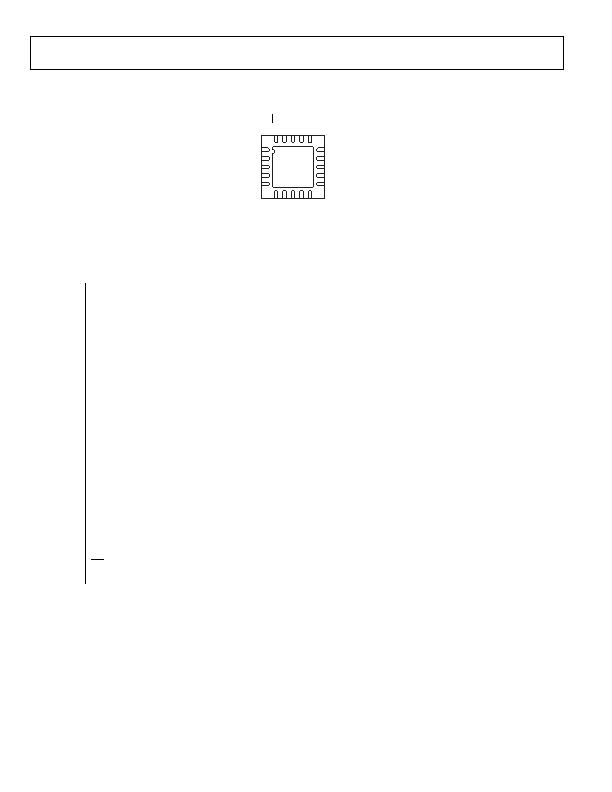
PIN CONFIGURATION AND FUNCTION DESCRIPTIONS
ADP5042
TOP VIEW
(Not to Scale)
NOTES
1. EXPOSED PAD SHOULD BE CONNECTED TO AGND.
2. NC = NO CONNECT. DO NOT CONNECT TO THIS PIN.
14
13
12
1
3
4
VOUT2
15 WSTAT
VIN2
WDI2
11 VOUT1
NC
VIN3
2
VOUT3
EN3
5
nRSTO
Figure 2. Pin ConfigurationView from Top of the Die
Table 8. Preliminary Pin Function Descriptions
Pin No.
Mnemonic Description
1
NC
Do not connect to this pin.
2
VOUT3
LDO2 Output Voltage and Sensing Input.
3
VIN3
LDO2 Input Supply (1.7 V to 5.5 V).
4
EN3
Enable LDO2. EN3 = high: turn on LDO2; EN3 = low: turn off LDO2.
5
nRSTO
Open-Drain Reset Output, Active Low.
6
AVIN
Regulators Housekeeping and Supervisory Input Supply (2.3 V to 5.5 V).
7
VIN1
Buck Input Supply (2.3 V to 5.5 V).
8
SW
Buck Switching Node.
9
PGND
Dedicated Power Ground for Buck Regulator.
10
EN1
Enable Buck. EN1 = high: turn on buck; EN1 = low: turn off buck.
11
VOUT1
Buck Sensing Node.
12
WDI2
Watchdog 2 (Long Timeout) Refresh Input from Processor. Can be disabled only by factory option.
13
VIN2
LDO1 Input Supply (1.7 V to 5.5 V).
14
VOUT2
LDO1 Output Voltage and Sensing Input.
15
WSTAT
Open-Drain Watchdog Timeout Status. WSTAT = high: Watchdog 1 timeout or power-on reset; WSTAT = low:
Watchdog 2 timeout. Auto cleared after one second.
16
EN2
Enable LDO1. EN2 = high: turn on LDO1. EN2 = low: turn off LDO1.
17
MODE
Buck Mode. MODE = high: buck regulator operates in fixed PWM mode; MODE = low: buck regulator operates
in pulse skipping mode (PSM) at light load and in constant PWM at higher load.
18
WMOD
Watchdog Mode. WMOD = low: Watchdog 1 normal mode; WMOD = high: Watchdog 1 cannot be disabled by
a three-state condition applied on WDI1.
19
WDI1
Watchdog 1 Refresh Input from Processor. If WDI1 is in high-Z and WMOD is low, Watchdog 1 is disabled.
20
MR
Manual Reset Input, Active Low.
TP
AGND
Analog Ground (TP = Thermal Pad). Exposed pad should be connected to AGND.
发布紧急采购,3分钟左右您将得到回复。
相关PDF资料
ADT6402SRJZ-RL7
IC TEMP SENS TRIP PT PP SOT-23-6
ADT6501SRJZP085RL7
IC TEMP SENSOR MICROPWR SOT23-5
ADT7302ARTZ-500RL7
IC SENSOR TEMP 13BIT DGT SOT23-6
ADT7310TRZ
IC TEMP SENSOR 16BIT SPI 8SOIC
ADT7461AARMZ-R
IC TEMP SENSOR DGTL 2CH 8-MSOP
ADT7461ARMZ-2R
IC TEMP SENSOR DGTL 2CH 8-MSOP
ADT7463ARQZ-REEL
IC REMOTE THERMAL CTRLR 24-QSOP
ADT7476AARQZ-R
IC REMOTE THERMAL CTLR 24QSOP
相关代理商/技术参数
ADP5042CP-1-EVALZ
功能描述:电源管理IC开发工具 Output Buck Regulator + Dual Fixed Eval RoHS:否 制造商:Maxim Integrated 产品:Evaluation Kits 类型:Battery Management 工具用于评估:MAX17710GB 输入电压: 输出电压:1.8 V
ADP5042CP-2-EVALZ
功能描述:电源管理IC开发工具 Output Buck Regulator + Dual Fixed Eval RoHS:否 制造商:Maxim Integrated 产品:Evaluation Kits 类型:Battery Management 工具用于评估:MAX17710GB 输入电压: 输出电压:1.8 V
ADP5043ACPZ-1-R7
功能描述:IC REG DL BUCK/LINEAR 20LFCSP RoHS:是 类别:集成电路 (IC) >> PMIC - 稳压器 - 线性 + 切换式 系列:- 标准包装:2,500 系列:- 拓扑:降压(降压)同步(3),线性(LDO)(2) 功能:任何功能 输出数:5 频率 - 开关:300kHz 电压/电流 - 输出 1:控制器 电压/电流 - 输出 2:控制器 电压/电流 - 输出 3:控制器 带 LED 驱动器:无 带监控器:无 带序列发生器:是 电源电压:5.6 V ~ 24 V 工作温度:-40°C ~ 85°C 安装类型:* 封装/外壳:* 供应商设备封装:* 包装:*
ADP5043CP-1-EVALZ
功能描述:BOARD EVAL ADP5043CP-1 RoHS:是 类别:编程器,开发系统 >> 评估板 - DC/DC 与 AC/DC(离线)SMPS 系列:* 产品培训模块:Obsolescence Mitigation Program 标准包装:1 系列:True Shutdown™ 主要目的:DC/DC,步升 输出及类型:1,非隔离 功率 - 输出:- 输出电压:- 电流 - 输出:1A 输入电压:2.5 V ~ 5.5 V 稳压器拓扑结构:升压 频率 - 开关:3MHz 板类型:完全填充 已供物品:板 已用 IC / 零件:MAX8969
ADP50450003CBZR
制造商:Analog Devices 功能描述:
ADP50460008CBZR
制造商:Analog Devices 功能描述:
ADP5050
制造商:AD 制造商全称:Analog Devices 功能描述:5-Channel Integrated Power Solution with Quad Buck Regulators and 200 mA LDO Regulator
ADP5050ACPZ-R7
功能描述:PMIC 解决方案 Adj 12V uPMU 4Buck+LDO+I2C I/F
RoHS:否 制造商:IDT 安装风格: 封装 / 箱体: 封装:
